Friday, October 20, 2017

DAUGHTER BOARD FOR RF430FRL152H

RF430FRL152 is the NFC SOC by Texas Intrument. The SoC comes with a MSP430 core 16 bit processor, with 2KB of FRAM for user code. It contain 8KB of builtin ROM code.  The chip has in built temperature sensor and current sources for external sensors.
IIC for digital sensor interfaces and internal energy harness and also the voltage doubler. The IC operates with 1.5 voltage with maximum of 1.65 voltage.


Wednesday, September 27, 2017

DEBUGGING ON TMP112 INTERFACE WITH MSP430FR5969 #20102016

  • Temperature sensor was successfully interfaced with the processor and giving the current temperature data in degree Celsius.
  • Minimum resolution of the current sensor is 0.0625 degree C, and accurate up to 0.5 degree C up to 65 degree C and 1 degree C beyond.

  • The picture shows the temperature at the time of measurement highlighted, upto precision of 3 digits after decimal.
  • ‘a’ section of the waveform is the address of temperature sensor,
    ‘b’ section is the internal temperature register address, which is all zero.
    ‘c’ and ‘d’ are the temperature value in binary(16 bits).

  • Changes made in Code
A) After software reset of IIC some delay is required, this issue took most of the time.
B) Set the IIc master mode with synchronous setting of 400Khz of data rate.
C) Low power implementation in current sensor for the long term battery life.
D) This configuration keeps the sensor in sleep mode and only waking up when temperature is need to be measures and then sent to sleep again. 


Saturday, September 23, 2017

TMP112 INTERFACING WITH MSP430 MICROCONTROLLER #19102016

TMP112, temperature sensor by Texas Instrument, with very interesting features as
a) SOT563 Pacakge (1.6mm x 1.6mm) is 68% smaller than SOT23.
b) Accuracy of 0.5C
c) Low quiescent of 10uA active and 1uA sleep
d) 12 bit resolution (0.0625C)
e) Supply range 1.4 to 3.6V


The i2c algorithm that we are using to sense the temperature sensor is as

A)      Should be in reset state while changing some register content. (check in datasheet)
B)      Set the IIc master mode with synchronous setting.
C)      Set IIc clock equal to sub master clock
D)     Set some divider smclk/x = 100khz (can be varied as per requirement up to 400khz)
E)      Set the slave address in 7 bit format
F)      Disable or enable the interrupts
G)     Disable the reset state


a)      Again put in reset mode
b)      Generate the stop condition after transmission of 1 byte automatically.
c)      Disable reset mode
d)      Send the start condition, it will also send the slave address.
e)      Wait until transmission is finished
f)      Send the register we need to read from and wait till transmission is done
g)      Set IIC write operation in receiver mode to generate auto stop after two bytes are received.
       TMP112 sensor gives 16 bits of data
h)      Setup for repeated start
i)       Receive two bytes of data
j)       Convert according to the formula

 (50°C) / (0.0625°C / LSB) = 800 = 320h = 0011 0010 0000
 0011 0010 0000 = 320h = 800 × (0.0625°C / LSB) = 50°C

(|–25°C|) / (0.0625°C / LSB) = 400 = 190h = 0001 1001 0000 Two's complement format: 1110 0110 1111 + 1 = 1110 0111 0000

Tuesday, June 27, 2017

TUNING OF PCB ANTENNA FOR NFC CIRCUITS #17102016

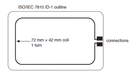
For testing the antenna, we first made a loop antenna as per reference to ISO/IEC 7810 ID-1 outline as per the figure shown below with dimension given.
o   Then an experimental setup was made as shown below:


o   The signal generator is connected across the antenna we had designed and then this PCB antenna board was placed on the loop antenna, which was connected to oscilloscope to view the frequency, and the voltage induced in the loop antenna (with 50Ω input resistance).
o   While measuring the inductance of the antenna alone using LCR meter, we observed it to be 3.6 micro henry at 1mhz. Since our LCR meter can only measure up to 1uH, we used hit and trial method using convergence of the resonant frequency by calculating the tuning capacitor and inductor each time with the frequency that was seen on oscilloscope.

o   The initial tests and results made showed the result as:
Antenna + 30pf(NFC ic equivalent) capacitor in parallel
At 26mhz, induced voltage = 150mv
At 15.8mV, induced voltage = 50mv
At 43.8mhz, induced voltage = 80mv
Antenna + 30pf(NFC ic equivalent) +10pf(tuning capacitor) in parallel
At 27.6mhz, induced voltage = 474mv


o  From the above, result we figured out that the tuning of capacitance leads to increase in the induced voltage as well resulting the increased efficiency. But the problem was the antenna was still tuned to 27.6Mhz, that is around next order of our required frequency 13.56mhz. i.e double than the required.

o   In above picture, we can see the voltage induced in loop antenna from our designed antenna when initially only some random tuning capacitor of 40pf was placed and the frequency was not tuned yet.
o   So to tune the antenna to the 13.56mhz, we first calculated the inductance at the frequency at which the highest voltage was induced and by placing value of capacitance as the used capacitor value. For this  


      formula was used.
o   For initial tuned frequency = 27.6mHz, tuning capacitor = 40pf, resultant calculated inductance was 0.83131uH.
o   So, in next iteration we used frequency = 13.56mhz, inductance = 0.831831uH, the calculated capacitor was 165.71pf.
o   So, next time we put this capacitor in the circuit. In continuing this iteration for several run, we got the calculated capacitor as 400pf and actual used capacitor as 380pf to get the resonant frequency at 13.56mhz and the maximum voltage induced.
o   Below is the maximum induced voltage at our required 13.56 mhz signal. But the efficiency is still low so which seems to be enough to get signal but not power up the circuit. (further study should be done on knowing about if this induced signal is enough or not as well as increase the efficiency)

    Induced signal on loop antenna         input signal (13.56mhz @ 5V p-p)

o   We also checked our designed antenna as receiver and the previously available 13.56mhz signal generator. The setup and response is shown in figure below.


o   Here we can see almost 3V was induced in our designed antenna.
We need to further study about antenna design, antenna tuning and antenna testing (use of network analyzer, use of antenna design software etc) and implement in our next version board.

Monday, February 6, 2017

ANTICOLLISION STEPS IN NFC ISO14443B

Anticollison Steps in ISO 14443B
o   ISO 14443B (TYPE 2), has two main components reader (PCD) and tag (PICC).
o   At first PCD uses the anti-collision sequence for checking for multiple PICCs.
o   Steps
§  PCD sends REQB command with N where N is number slots defined for anti collision.
§  PICC receives REQB and check for N

  • If N is 1 then returns ATQB (Answer to Request type B)
  • If N is greater than 1  then random number R is generated
  • If R is 1 then sends ATQB
  • If R is not 1 then it wait until slot marker sent by PCD is matched

SIGNALLING IN NFC ISO 14443B
o   Uses the frequency of 13.56MHz as major carrier.
o   Sub carrier if 847.5 KHz is used for carrying data.
o   Signal from PICC to PCD is load modulated and used different signaling than from PCD to PICC.

PCD to PICC signaling
o   Uses 10%(8 to 14% practically) amplitude modulation index, ie there is always a presence of 13.56MHz carrier
o   Uses the NRZ encoding for the data
o   The signal generated from the smart phone as captured shows modulation index of 15%
o   Uses BPSK (Binary Phase Shift Keying) modulation
o   Encoding is NRZ-L for the data.
o   Each of the bit is 8 sub carrier period long.

Wednesday, January 11, 2017

SOFTWARE BASED UART ON ANY CONTROLLER

UART are very easy way for communication in electronics, it is used mostly in any where. UART are available in any micro controllers and very easy to use and understand. 
Sometimes in some controllers we may required some extra UART than available in hardware, in such case we can use software based UART. The details of USART communication is out of scope of this post. 

The code is running on MSP430FR5969, the device is running on 4 MHz DCO. The following code do not utilized any kind of interrupt and strictly depended on polling. While receiving the data, it uses while statement for the start bit. But this code be easily be made efficient using techniques like interrupts and also using PT thread technique. This just gives a basic implementation for the newbies.

The setup is as


Here macros are used for making the code simpler, following are the snippets of the functions.

#define settxoutput P1DIR |= BIT4  //SET AS TX OUTPUT PORT 1 BIT 4
#define highontx P1OUT |= BIT4 //SET OUTPUT HIGH ON TX
#define setlowontx P1OUT &= ~BIT4 //SET OUTPUT LOW ON TX

#define setrxinput P1DIR &= ~BIT3 //SET AS RX INPUT PORT 1 BIT 3
#define isrxhigh P1IN&BIT3

#define baudrate 9600
#define Bittime 4000000/baudrate // one bit time in uS
#define bittime Bittime - 40
#define rbittime Bittime - 40

void tx8_uart(unsigned char data8){
unsigned char i;
setlowontx;
__delay_cycles(bittime); //since frequency of operation is 1mhz its 1us
for( i = 0;i < 8 ; i++){
if( ( (data8>>i) & 0x01) == 0x01 )
highontx;
else
setlowontx;
__delay_cycles(bittime);
}
highontx;
__delay_cycles(bittime);
}


unsigned char  rx8_uart(){
unsigned char data8=0;
int i;

while(isrxhigh); //start bit is 0

__delay_cycles(rbittime);
__delay_cycles(rbittime/2);//taking sample at mid time

for( i = 0;i<8;i++){
if( /*i%2 == 0*/ isrxhigh ){
data8 += (1<<i);
//P1OUT |= BIT7;
}
else{
data8 = data8;
// P1OUT &= ~BIT7;
}
__delay_cycles(rbittime);
}

if( isrxhigh ){
__delay_cycles(rbittime/2);
return data8;
}else{
__delay_cycles(rbittime/2);
return 0x00;
}
}

Monday, July 25, 2016

P10 LED MATRIX BOARD DISPLAY

Here in this project I have used 12 P10 led matrix board in array of 4 horizontal and 3 vertical ie 4 columns and 3 row.
All displays are cascaded ,while last one become the origin or 0,0.

You need a long flat cable of 16 pin connector for connecting the display on different line as suggested in the figure.
I have used the DMD library by freetronics.
First I have planned to display time temperature one the first line, display two messages scrolling in line two and three.
I have used LM35 as temperature sensor which gives 10mV per degree change in celsius scale and used 1.1V as ADC reference for maximum resolution. 
DS1307 as RTC with IIC interface, but the problem is whenever is use DMD with IIC, I dont know why the time value of RTC is not stable its always changing like it gives right time for 3 or 5 times and then 165 165 and 85. May be due to some conflict on resources couldnt really figure out.
Solve this problem using two controller using one as just display drivers and second sending all data of temperature, time, font, writing message , reading message and saving message and controlling the speed of the message scroll.
Here's the link to the code final code https://github.com/kieran-shrestha/led_notice_board

Saturday, July 9, 2016

INTERFACING ADC OF AVR MICROCONTROLLER

The following is the code for using the internal 10 bit ADC of AVR microcontroller.
The code is written for ATMEGA328 with system clock of 16MHZ.
The code uses standard c header files for using printf function and then print the content in serial uart of the microcontroller.

Sunday, June 26, 2016

ATMEGA328P UART0

CONNECTION CONNECT RX AND TX TO TX AND RX OF OTHER DEVICE

//This define the system frequency
#define F_CPU 16000000UL

//Including the required files
#include <avr/io.h>
#include <util/delay.h>

Sunday, June 12, 2016

LCD INTERFACING 8 BIT MODE

Circuit connection is 
RS => PB0
RW => PB1
EN => PB2
D0-D3 =>PORTD 0 TO 3
D4-D7 => PORTC 0 TO 3

READING A GPIO

Circuit diagram includes using PORTB5 as output to toggle a LED and PORTC5 for input with button connected to ground.

BLINKING A LED

Circuit diagram includes connecting a LED with resistor in series in PORTB5, its digital 13 on Aruino.

Blink LED method 1

#define F_CPU 16000000

#include <avr/io.h>
#include <util/delay.h>

int main(void)
{
   
DDRB |= (1 << PORTB5);
    while (1)
    {
PORTB |= (1 << PORTB5);
_delay_ms(200);
PORTB &= ~(1<< PORTB5);
_delay_ms(100);

    }
}

Thursday, July 23, 2015

TERMS EXPLAINED IN CLASS D AMPLIFIERS

Class D amplifiers are one most used and popular amplifier due to efficiency, theoretically class d amplifiers are 100 percent efficient. But this cannot be achieved practically as no device is 100 percent efficient. Though class d amplifiers reach more than 90% of efficiency if designed very carefully.
Understanding class d amplifiers are very much simple if you are familiar with the Switch mode power supply or commonly called SMPS or switching supply.
Input for the class d amplifier is first modulated either using Pulse Width Modulation ie PWM or sigma Delta modulates. Order of modulation starts generally from two and can reach as higher as 5 or even higher.
Class d amplifier can either be half bridged which requires dual power supply or full bridge and can be powers with single power supply. The problem with full bridge is that it requires more hardware or switching MOSFET which decrease its efficiency.
Another thing that make the class d amplifiers better is bridge tied load configuration or bridging multiple amplifiers so that its output power can be doubled. In bridge tied load configuration two half bridge amplifiers as bridged so that its output is doubled and the power for this configuration should be dual Power supply.
What is happening in class d amp is the modulated PWM is turning on and off the MOSFET bridge. during this MOSFETs ate switched on alternately. But if two of the MOSFETs on high side is turned on a pop sound can be created which may be very annoying. Also if there is delay between the next switching sequence the there might be dead sound between the sound.

Tuesday, May 26, 2015

BROKEN YOUR AVR CHIP?

While working the avr for the first time it is always confusing while programing the fuse bits as wrong configuration of this can damage the chip or may be lock the chip so you cannot program it normally.

If your making a bare bone arduino or burning arduino boot loader the fuse bits if programmed wrong can lock the device. This often happens due to some of the following fuse bits.
A. First thing you are being greedy of that single reset pin to use it as gpio. But you will be programming it only once as after that fuse setting to use reset as gpio avr can't be programmed using ISP as ISP programming requires external reset operations . so you need to do the high voltage programming either serial or parallel.
For the he high voltage programming you can consult the avr data sheet where it is described crystal clear and also there are many tutorials available online for this problem.


Also choosing external clock source can also result avr to not work using ISP in this case high voltage programming can be used or a external TTL clock should be used for the programming.

Heres the line copied from datasheet of high voltage programming. 

The following algorithm puts the device in Parallel (High-voltage) Programming mode:

1. Set Prog_enable pins listed in Table 28-12 on page 290 to “0000”, RESET pin to 0V and
VCC to 0V.

2. Apply 4.5V - 5.5V between VCC and GND.
Ensure that VCC reaches at least 1.8V within the next 20μs.

3. Wait 20μs - 60μs, and apply 11.5V - 12.5V to RESET.

4. Keep the Prog_enable pins unchanged for at least 10μs after the High-voltage has been
applied to ensure the Prog_enable Signature has been latched.

5. Wait at least 300μs before giving any parallel programming commands.

6. Exit Programming mode by power the device down or by bringing RESET pin to 0V.

If the rise time of the VCC is unable to fulfill the requirements listed above, the following alternative
algorithm can be used.

1. Set Prog_enable pins listed in Table 28-12 on page 290 to “0000”, RESET pin to 0V and
VCC to 0V.

2. Apply 4.5V - 5.5V between VCC and GND.

3. Monitor VCC, and as soon as VCC reaches 0.9V - 1.1V, apply 11.5V - 12.5V to RESET.

4. Keep the Prog_enable pins unchanged for at least 10μs after the High-voltage has been
applied to ensure the Prog_enable Signature has been latched.

5. Wait until VCC actually reaches 4.5V - 5.5V before giving any parallel programming
commands.

6. Exit Programming mode by power the device down or by bringing RESET pin to 0V.


Monday, May 25, 2015

PIC vs AVR #30 #2

This is the second part of the pic and avr. One of the benefit of the avr is programming.

For the programming or firmware development avr gives AVR studio which is a very good IDE and most important for beginner is it's free. AVR studio gives most of the libraries for their micro controllers and also for the different boards made by ATMEL. 

Also one of the most important benefit that you get from AVR's 8 bit controllers is arduino. Arduino is a open source project. You can visit www.arduino.cc for more informations. Its based on AVR and most popular is ATMEGA328. You can use almost any other microcontrollers. 

For the beginners who are not so into the hardware of microcontroller thing and also with the hardware or internal things of the controller. Arduino make programming so easy that any can interface any hardware to it.

PIC on the other hand also provide their own IDE, MPLAB X , it uses a separate compiler. The bad thing is its not free. There's also a free version which does all the job done for the beginner but what the free version is not giving us is maximum code optimization . Paid version of MPLAB  gives the maximum optimization which is more that 50 % of the code size of the free version. 

PIC also provide some of the libraries for its users , also MIKRO C gives some simple programming interface for the PIC which is the third party PIC IDE. 

These are some of the things to compare between the PIC and AVR. Further on its on you to choose between PIC or AVR. 

Saturday, May 23, 2015

PIC VS AVR MICROCONTROLLER #29 #1

For the starters it is always the question in mind whether to use PIC microcontroller or AVR microcontroller. PIC manufacutred by MICROCHIP and AVR by ATMEL is beginner level 8 bit micorcontrollers which every beginner use.

If your starting a project or starting to learn some more on controllers which to follow. I list out some of my points on both controllers their pros and cons.

Moving on to PIC ,  PIC's 8 bit series 16F and 18F are the most popular one. These PIC controllers are available in package like SSOP,SOIC,DIP,QFN,QFP. 

If your project is power sensitive PIC is the best. PIC's nanoWatt XLP series have very low power. They in even go to micro Ampere current range when in Deep Sleep. Though AVRs got the power control like sleep, stand by modes but PIC is better than AVR in this matter.

Other benefit that PICs got is PIC has more features in chip than AVR. They have more peripheral fetures and control than AVR . PICS got many standard like ECAN, more CCP and ECCP channels and controls more AD converter channels than AVR. 

Its not like AVR got no such feature AVR's also got the same feature but AVR's got less flexibility in these things. 

Thing in which AVR dominates PIC is in my case TIMERS, In AVR timers got more controls than in PIC. Handling timers in AVR is always easy than PIC.

In term of cost both are same , but some PICs are cheaper in compared to AVR. 


Friday, November 28, 2014

CHOOSING AND DRIVING A MOSFET #1 #28

MOSFETS are some what confusing than the Bipolar Juntion Transistors BJT or simply transistors. MOSFETS (Metal Oxide Semiconductor Field Effect Transistors) are voltage controlled current source (VCCS) while BJT are current controlled current source. One of the well known relation for the transistor is Ic = B Ib. Where  B is beta or Hfe current gain of the transistor and is usually >10 for high power transistors and >100 for small signal transistors. 
So controlling the current flowing in the Base of the transistor one can control the output current flowing from the collector to emitter or from emiter  to collector in case of NPN and PNP transistors. 
High power transistors require more silicon space in comapre to the same space with the MOSFETS.


In case of Mosfets, they are of N channel and of P channel. Both have its own advantages and dis advantages. But the common of the Mosfets are that both the Mosfets only start conduction when the voltage in its GATE terminal exceeds some voltage level than that of the voltage level in source, which is called Vgs = Vth = Gate threshold voltage. Understanding this voltage level is very important for the design withe Mosfets. Vgs voltage from gate to source is position in the case of the N channel but for the P channel its in negative. But it is still easy to drive the gate of the Mosfets.


N channel have some advantages as they have electrons as their carrier and they have more mobility so the N channel mosfets have very low ON resistance called Rds than the P channel mosfet with same size of die or silicon and this reason need of more silicon space also make P channel mosfet more expensive. 

Wednesday, November 5, 2014

SVN VERSION CONTROL IN ALTIUM #27

Version control in makes any project very easy to manage and work with different versions of the same projects and makes modifications and make easy management of all the versions and storing of all the versions.
In Altium, it has got its own version control and also SVN external version control.

THIS TUTORIAL IS ONLY FOR THE VERSION CONTROL OF THE PROJECTS IN LOCAL COMPUTER ONLY.

Step 1: Make new PCB project.


Step 2: Then go to preferences of ALTIUM  and navigate to Data Management and Version Control
and check the User external Suberversion Radio button and check on SVN-Suberversion check box. Or click on Auto Detect.


Step 3: Now click on Design Repositories and click on Create New and Click on SVN.


Step 4: Name Repository some name like "MyRepo" and in location choose the folder where you work. Mine is "altiumrepo". Then Hit OK.
The status will be green if everythings OK.


Step 5: Now on project right click and choose version control and add project to version control.


Step 6: Choose the Repo and Hit OK.


Now we can comit the project or inidivual file from the same menu by right clicking it . For check out go to storage manager and right click and click on revert on specified file or project.


Monday, October 27, 2014

FTDI Bricking all the non genuine FTDI chips #26


FTDI are used for easy USB connections in microcontroller and are widely used.  FTDI updating drivers in windows machine for detecting the counterfeit Ics and then re writing their internal eeprom’s Product id to zero so that no machine can read the usb device again. They are bricking the chips and no use for  further.
FTDI been hitting their own market and all the users are real mad. Here’s the video on EEVLOG. https://www.youtube.com/watch?v=eU66as4Bbds


Friday, October 10, 2014

ENABLE LARGE CROSS HAIR IN ALTIUM DESIGNER #25

We have the default small cursor as

Then to change to large cursor or cross hair.


Step 1 :
Go to preferences. DXP -> Preferences or Tools -> Preferences


Step 2:
Navigate to PCB editor -> General.


Step 3:
Click on the drop down menu with small 90 chosen.


Step 4:
Choose large 90 and hit enter or OK.

Then its done.